Hardware
What to connect between your MCU and an AS5047U, with which bus settings, and how to power it and place the magnet.
All values here come from the AS5047U datasheet (DS000637, v1-01, 2020-12-16). Figure numbers refer to it.
Pins
TSSOP-14 (Figure 3 and 4). Directions are seen from the chip.
| Pin | Name | Direction | Function | If unused |
|---|---|---|---|---|
| 1 | CSn |
in | SPI chip select, active low | Pull up |
| 2 | CLK |
in | SPI clock | Pull down |
| 3 | MISO |
out | SPI data out | Leave open |
| 4 | MOSI |
in | SPI data in | Pull down |
| 5 | TEST |
Test pin | Always connect to GND | |
| 6 | B |
out | Incremental signal B | Leave open |
| 7 | A |
out | Incremental signal A | Leave open |
| 8 | W/PWM |
out | Commutation W, or PWM angle | Leave open |
| 9 | V |
out | Commutation V | Leave open |
| 10 | U |
out | Commutation U | Leave open |
| 11 | VDD |
power | Supply; 5 V into the on-chip LDO, or 3.3 V | |
| 12 | VDD3V3 |
power | LDO output (1 µF to GND), or the 3.3 V supply | |
| 13 | GND |
power | Ground | |
| 14 | I/PWM |
out | Index pulse I, or PWM angle | Leave open |
Digital inputs must never float. The ABI, UVW and PWM outputs drive at most 4 mA at 5 V and 2 mA at 3.3 V into at most 50 pF.
Bus settings
| Setting | Value |
|---|---|
| Mode | SPI mode 1: CPOL = 0, CPHA = 1. The chip samples MOSI on the falling edge of CLK |
| Bit order | MSB first |
| Clock | Up to 10 MHz (tclk ≥ 100 ns) |
| Frame | 16 bits (reads only, no CRC), 24 bits (CRC-8) or 32 bits (CRC-8 and a PAD byte) |
| Chip select | Active low, one frame per low period. The chip executes the frame on the rising edge of CSn |
| Reply | The data for a read arrives during the next frame |
| Driver default | 16-bit frames (AS5047U_CFG::DEFAULT_FRAME_FORMAT); writes always go out as 24-bit frames |
SPI protocol shows the bits of each frame, the CRC and the read and write sequences.
Timing
Figure 19. The two 350 ns limits are the ones a port can break: CSn low to the first clock edge, and CSn high between two frames. A hardware chip select usually meets them with one or two clock cycles of set-up and hold; a GPIO chip select toggled right next to the transfer may not.
| Symbol | Parameter | Min | Max | Unit |
|---|---|---|---|---|
| tL | CSn falling edge to first CLK rising edge | 350 | ns | |
| tclk | Clock period | 100 | ns | |
| tclkH, tclkL | Clock high and low time | 50 | ns | |
| tH | Last CLK falling edge to CSn rising edge | tclk / 2 | ns | |
| tCSn | CSn high time between frames | 350 | ns | |
| tMOSI | MOSI valid before the clock edge | 20 | ns | |
| tMISO | Clock edge to MISO valid | 51 | ns | |
| tOZ | CSn rising edge to MISO high-impedance | 10 | ns |
The 350 ns minimums come from synchronizing to the internal 9 MHz clock (2 × tCLK_SYS + 10 ns).
sequenceDiagram
    participant H as Host (driver)
    participant C as AS5047U
    H->>C: frame 1: read ANGLECOM (0x3FFF)
    C-->>H: reply to the previous frame (discarded)
    H->>C: frame 2: read NOP (0x0000)
    C-->>H: ANGLECOM, warning and error bits, CRC
    H->>C: frame 3: read ERRFL (0x0001)
    C-->>H: NOP reply (discarded)
    H->>C: frame 4: read NOP
C-->>H: ERRFL (reading it clears it on the chip)Power
| Mode | Supply pins | Temperature | Noise (rms) |
|---|---|---|---|
| 5 V | VDD 4.5 V to 5.5 V; VDD3V3 is the LDO output, 1 µF to GND | −40 °C to 150 °C | 0.068° |
3.3 V, NOISESET = 0 |
VDD and VDD3V3 tied, 3.0 V to 3.6 V | −40 °C to 125 °C | 0.068° |
3.3 V, NOISESET = 1 |
VDD and VDD3V3 tied, 3.0 V to 3.6 V | −40 °C to 150 °C | 0.082° |
The LDO powers nothing but the chip. Select NOISESET with Set150CTemperatureMode().
- Supply current is at most 16 mA. Put 100 nF from VDD to GND in both modes.
- The first valid angle is available at most 10 ms after VDD rises above its minimum (tpon).
- The logic levels follow VDD: VIH ≥ 0.7 × VDD, VIL ≤ 0.3 × VDD. In 5 V mode a 3.3 V MCU needs a level shifter on CLK, MOSI and CSn (0.7 × 4.5 V = 3.15 V), and MISO swings up to VDD.
- Absolute maximum: 7.0 V on VDD, 5.0 V on VDD3V3.
- OTP programming needs 4.5 V to 5.5 V (5 V mode) or 3.3 V to 3.5 V (3.3 V mode), up to 100 mA, at 5 °C to 45 °C. See OTP programming.
GetDiagnostics().bits.VDD_mode reads 1 in 5 V mode and 0 in 3.3 V mode.
Magnet
| Parameter | Value |
|---|---|
| Type | Diametrically magnetized (two poles across the diameter), centered on the package axis |
| Field at the die | 35 mT to 70 mT, orthogonal component, along a circle of 1.1 mm radius |
| Datasheet reference magnet | N35H, 8 mm diameter, 3 mm thick |
| Speed | Up to 28000 rpm |
| Accuracy (optimal placement) | ±0.8° at 25 °C, ±1° over −40 °C to 150 °C (maximum non-linearity) |
The AGC keeps the field magnitude constant while the field is in range; AGC at 0 or 255 means the magnet is too close or too far. Read ERRFL or AGC regularly: the datasheet requires one of them to be read for the AGC loop to work as specified.
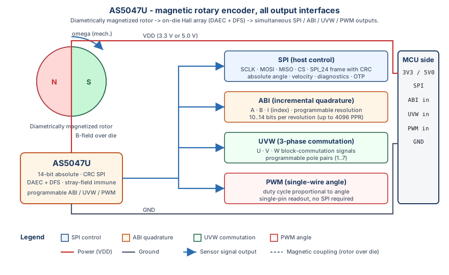
Outputs other than SPI
| Output | Pins | What it carries | Driver calls |
|---|---|---|---|
| ABI | A, B, I/PWM | Quadrature, 25 to 4096 pulses per turn; index once per turn, 3 LSB or 1 LSB wide. All high during start-up | SetABIResolution(), SetIndexPulseLength() |
| UVW | U, V, W/PWM | Hall-sensor emulation for 1 to 7 pole pairs. All low during start-up | SetUVWPolePairs() |
| PWM | W/PWM or I/PWM | 12-bit angle in a frame of 4119 PWM clocks of 444 ns typical (about 1.83 ms) | ConfigureInterface(..., pwm) |
The PWM pin is W when ABI is active and I when UVW is active (SETTINGS2.UVW_ABI). The PWM angle is not
dynamically compensated. Configuration has the combinations.
The examples' board
The ESP32 examples build for an ESP32-S3 (examples/esp32/app_config.yml) with the sensor on
SPI2: CS GPIO10, MOSI GPIO11, SCLK GPIO12, MISO GPIO13, mode 1 at 1 MHz. The assignment is in
esp32_as5047u_test_config.hpp.
Reference documents
| Document | What it is for |
|---|---|
| AS5047U datasheet | Pins, electrical limits, SPI frames, registers, OTP procedure |
| Application note AS5x47U Adaptive Filter (ams OSRAM) | Choosing K_min and K_max for the adaptive filter |